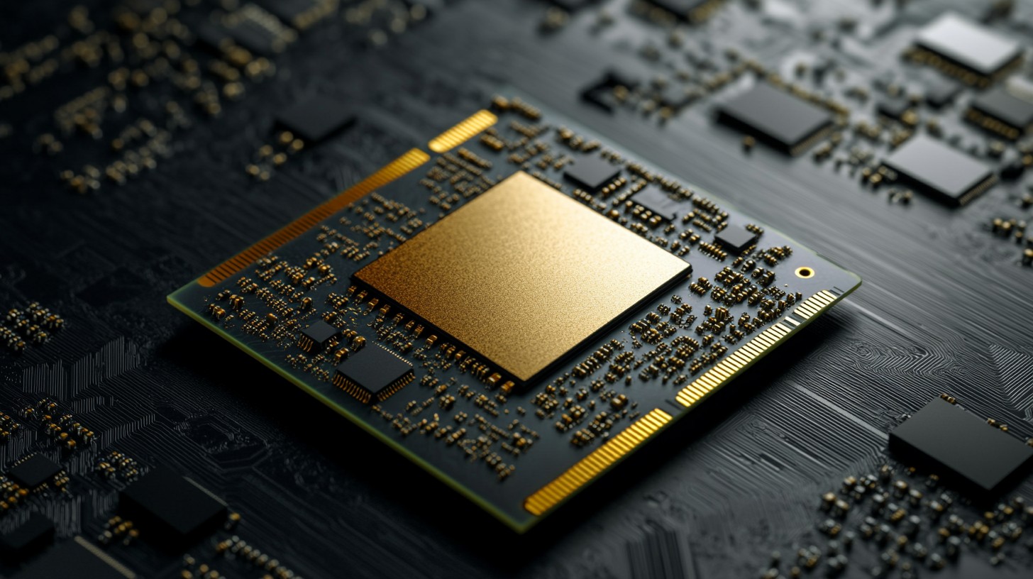
Every smartphone, laptop, and smart device in your life depends on one of humanity’s most remarkable inventions: the microprocessor. These tiny chips, often no bigger than your thumbnail, contain billions of transistors working in perfect harmony to power our digital world. Understanding how microprocessors work—from their creation out of ordinary beach sand to their role as the brain of every computing device—reveals one of science’s most fascinating stories. Let’s explore this incredible journey from raw silicon to the processors that run our modern lives.

The Foundation: Silicon from Sand
The story begins with something you’ve probably walked on countless times: sand. Specifically, silicon dioxide (SiO2), which makes up about 90% of the Earth’s crust and is the primary component of sand. Before we can understand how microprocessors work, we must first understand how we create the pure silicon that makes them possible.
Why Silicon?
Engineers don’t choose silicon randomly. It’s a semiconductor, meaning its ability to conduct electricity falls between conductors (like copper) and insulators (like rubber). This unique property is crucial because it allows us to control electrical flow with extreme precision. Silicon also has several practical advantages:
- Abundance: It’s the second most abundant element in Earth’s crust
- Stability: It forms a stable oxide layer that protects the chip
- Temperature tolerance: It works reliably across a wide temperature range
- Well-understood: Decades of research have perfected silicon processing techniques
From Sand to Pure Silicon
The transformation from sand to microprocessor-grade silicon is a multi-step purification process:
- Initial extraction: Manufacturers heat sand with carbon in an electric arc furnace at temperatures exceeding 2000°C (3600°F), producing metallurgical-grade silicon that’s about 98-99% pure.
- Chemical purification: The silicon undergoes the Siemens process, where it reacts with hydrochloric acid to form trichlorosilane gas. Workers then distill this gas and decompose it on heated silicon rods, creating polycrystalline silicon with 99.9999999% purity (that’s nine nines!).
- Crystal growing: Technicians melt the purified silicon and dip a seed crystal into it. As they slowly withdraw and rotate the seed, a single perfect crystal (called an ingot) grows. This Czochralski process creates cylindrical crystals up to 300mm in diameter and over a meter long.
- Wafer slicing: Precision saws slice the ingot into thin wafers, typically 0.775mm thick. These mirror-smooth wafers become the foundation for thousands of individual chips.
The Manufacturing Marvel: Building Billions of Transistors
Creating a modern microprocessor involves hundreds of precisely controlled steps. The process is so complex that a single chip might spend 2-3 months in fabrication and involve over 1,000 individual processing steps. This intricate manufacturing process is essential to how microprocessors work—each step builds the nanoscale architecture that enables computation.
Photolithography: Printing with Light
At the heart of chip manufacturing is photolithography, essentially an ultra-precise form of photography:
- Coating: Technicians coat the silicon wafer with a light-sensitive material called photoresist.
- Exposure: Ultraviolet light shines through a photomask (like a stencil) containing the circuit pattern. Modern chips use extreme ultraviolet (EUV) light with wavelengths of just 13.5 nanometers—about 1/10,000th the width of a human hair.
- Development: Developers chemically develop the exposed photoresist, removing either the exposed or unexposed areas (depending on the photoresist type).
- Etching: Chemical or plasma etching removes the exposed silicon, creating the desired pattern.
Manufacturers repeat this process dozens of times, building up layer upon layer of the chip’s intricate 3D structure.
Doping: Creating the Switches
Pure silicon isn’t enough. To create transistors, we need to modify its electrical properties through a process called doping:
- N-type doping: Adding elements like phosphorus or arsenic, which have extra electrons, creates regions with excess negative charge carriers.
- P-type doping: Adding elements like boron, which have fewer electrons, creates regions with positive charge carriers (actually holes where electrons should be).
Where P-type and N-type silicon meet, we create a PN junction—the fundamental building block of transistors and diodes.
Building Transistors: The Brain’s Neurons
Modern chips use MOSFET (Metal-Oxide-Semiconductor Field-Effect Transistor) technology. Each transistor acts as a tiny switch:
- Source and Drain: Two doped regions (either both N-type or both P-type)
- Channel: The region between source and drain
- Gate: A thin insulating layer separates this conductor from the channel
- Gate oxide: An incredibly thin layer of silicon dioxide (just atoms thick in modern chips)
When engineers apply voltage to the gate, it creates an electric field that either allows or blocks current flow between source and drain. This on/off behavior represents the 1s and 0s of binary computing.
Modern processors pack these transistors incredibly densely. A state-of-the-art 3-nanometer chip can contain over 20 billion transistors in an area the size of your fingernail.
Interconnects: Wiring It All Together
Transistors alone aren’t useful—they need to be connected in precise patterns. Modern chips use multiple layers of metal interconnects:
- Deposition: Technicians deposit thin layers of metal (typically copper or aluminum) using techniques like sputtering or chemical vapor deposition.
- Patterning: Photolithography defines where the metal should remain.
- Etching: Etching processes remove unwanted metal.
- Insulation: Layers of silicon dioxide or other dielectrics separate the metal layers.
High-end processors can have 15 or more layers of interconnects, creating a three-dimensional maze of connections.
How Microprocessors Work: From Transistors to Intelligence
Now that we’ve built billions of transistors and connected them, how do they actually compute? Understanding how microprocessors work requires examining the layers of logic that transform electrical signals into meaningful computation.
The Fundamental Logic: Boolean Gates
Engineers combine transistors to create logic gates that perform basic Boolean operations. These gates are the foundation of how microprocessors work at the logical level:
- NOT gate: Inverts the input (1 becomes 0, 0 becomes 1)
- AND gate: Outputs 1 only if both inputs are 1
- OR gate: Outputs 1 if either input is 1
- NAND, NOR, XOR: Combinations of the above
These simple gates are the foundation of all computation. By combining them in clever ways, we can build circuits that add, subtract, multiply, compare, and perform any computational task.
The Core Architecture
A microprocessor contains several key components:
1. Arithmetic Logic Unit (ALU)
The ALU performs mathematical operations (addition, subtraction, multiplication) and logical operations (AND, OR, NOT). Thousands of logic gates arranged in clever configurations like full adders and multipliers build it.
2. Control Unit
The control unit orchestrates everything. It fetches instructions from memory, decodes them, and coordinates the other components to execute them. Think of it as the conductor of an orchestra.
3. Registers
These are tiny, ultra-fast memory locations built directly into the processor. They temporarily hold data during active processing. Modern processors have dozens of registers, each typically 64 bits wide.
4. Cache Memory
Cache is high-speed memory built into the processor chip. It stores frequently accessed data and instructions, dramatically reducing the need to fetch information from slower main memory. Modern processors typically have three levels:
- L1 Cache: Smallest (32-64 KB) but fastest, split into instruction and data caches
- L2 Cache: Medium (256 KB-1 MB), still very fast
- L3 Cache: Largest (8-64 MB), shared between processor cores
5. Clock
The clock generates a rhythmic electrical pulse that synchronizes all operations. Modern processors run at speeds of 3-5 GHz, meaning billions of clock cycles per second.
The Instruction Cycle: Fetch, Decode, Execute
Every task your computer performs breaks down into this repetitive cycle. This is the fundamental answer to how microprocessors work at the most basic level:
- Fetch: The control unit retrieves the next instruction from memory using the address stored in the program counter (a special register).
- Decode: The processor decodes the instruction to determine what operation to perform and what data to use.
- Execute: The appropriate components (usually the ALU) perform the operation.
- Store: The processor writes results back to registers or memory.
This happens billions of times per second. A single simple program might involve millions of these cycles.
Pipelining: Doing Multiple Things at Once
Modern processors don’t wait for one instruction to complete before starting the next. Instead, they use pipelining, which is crucial to how microprocessors work efficiently:
Imagine an assembly line where the processor fetches one instruction while it decodes another and executes a third. Modern processors have pipelines 14-20 stages deep, allowing them to work on multiple instructions simultaneously.
Multiple Cores: Parallel Processing
Today’s processors contain multiple complete processing units (cores) on a single chip. A typical consumer processor has 4-16 cores, while high-end server processors can have 64 or more. Each core can execute its own instruction stream, allowing true parallel processing for multitasking and complex computations.
The Quantum Scale Challenge
As we push toward smaller transistors, we’re approaching fundamental physical limits:
The 3-Nanometer Barrier
Current state-of-the-art processors use transistors just 3 nanometers across. At this scale:
- Quantum tunneling: Electrons can “tunnel” through barriers that should block them, causing unwanted current leakage.
- Heat density: Packing more transistors into the same area generates tremendous heat.
- Manufacturing precision: Controlling features at the atomic scale requires unprecedented precision.
The Future: Beyond Silicon
Researchers are exploring alternatives to traditional silicon transistors. These innovations could change how microprocessors work in fundamental ways:
- Gate-all-around (GAA) transistors: Wrap the gate around the channel for better control
- Carbon nanotubes: Potentially faster and more efficient than silicon
- Graphene: A single layer of carbon atoms with remarkable electrical properties
- Quantum computing: Using quantum mechanical effects for computation (though this is fundamentally different from traditional processors)
The Economic Reality: Billion-Dollar Factories
The complexity of modern chip manufacturing reflects in the costs:
- A cutting-edge semiconductor fabrication plant (fab) costs $15-20 billion to build
- A single photomask set for a modern chip can cost $20 million
- The machines that create chips using EUV lithography cost over $150 million each
- Only a handful of companies (TSMC, Samsung, Intel) can afford to manufacture the most advanced chips
This economic reality is why chip manufacturing has become centralized in just a few locations worldwide, despite the global importance of semiconductors.
The Miracle in Your Pocket
The next time you check your smartphone or open your laptop, take a moment to appreciate the extraordinary technology at work. When you truly grasp how microprocessors work, the achievement becomes even more remarkable. Inside that small chip:
- Billions of transistors are switching on and off billions of times per second
- Electrons are racing through pathways measured in nanometers
- Multiple processor cores are coordinating complex parallel tasks
- Sophisticated algorithms are predicting what data you’ll need next
All of this started with ordinary sand, transformed through one of the most complex manufacturing processes ever devised, engineered to work at scales approaching individual atoms.
From the beaches to the clean rooms, from silicon crystals to binary logic, the microprocessor represents one of humanity’s greatest technological achievements—a testament to our ability to understand and manipulate the fundamental building blocks of matter to create something that appears, for all practical purposes, to think.
Conclusion
The journey from sand to silicon, from raw materials to working microprocessors, combines chemistry, physics, materials science, and engineering at scales both massive (billion-dollar factories) and minuscule (nanometer transistors). Understanding this process gives us appreciation not just for the devices we use daily, but for the incredible progress of human knowledge and capability. Learning how microprocessors work reveals the bridge between the physical and digital worlds.
As we continue pushing the boundaries of what’s possible, the fundamental principles remain the same: controlling the flow of electrons through carefully crafted silicon to perform the logical operations that power our digital world. Whether we’re developing new materials, new architectures, or entirely new computing paradigms, it all builds on this remarkable foundation—forged from the simplest and most abundant materials on Earth.
The microprocessor revolution continues to accelerate, with new innovations arriving constantly. While the specific numbers and technologies evolve, the fundamental principles of how microprocessors work—transforming sand into thinking machines—remain one of science and engineering’s most fascinating stories.